- 您现在的位置:买卖IC网 > Sheet目录3888 > PIC18C801T-I/PT (Microchip Technology)IC MCU ROMLESS A/D PWM 80TQFP
PIC18C601/801
DS39541A-page 106
Advance Information
2001 Microchip Technology Inc.
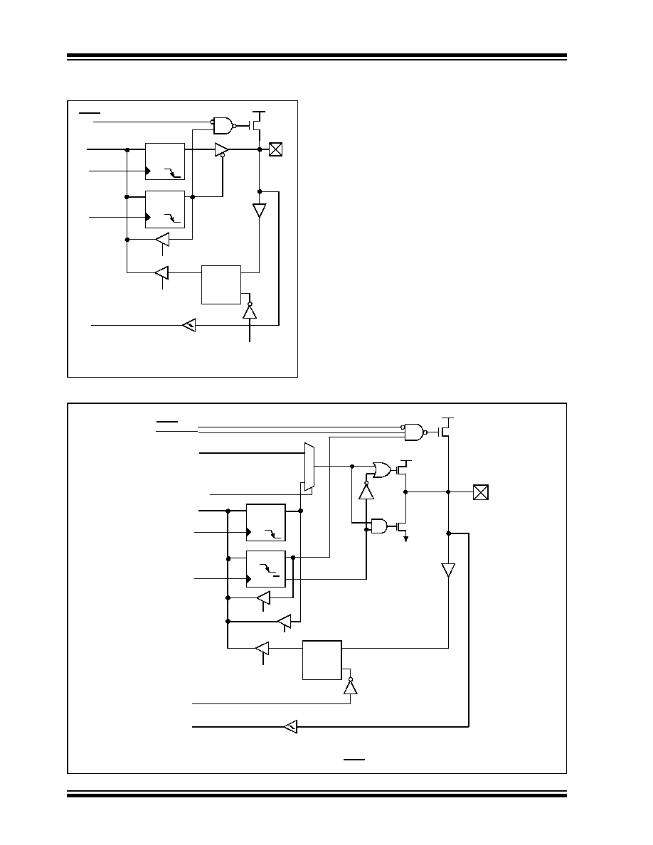
FIGURE 9-4:
RB2:RB0 PINS BLOCK
DIAGRAM
FIGURE 9-5:
RB3 PIN BLOCK DIAGRAM
Data Latch
RBPU(2)
P
VDD
Q
D
CK
Q
D
CK
QD
EN
Data Bus
WR Port
WR TRIS
RD TRIS
RD Port
Weak
Pull-up
RD Port
RBx/INTx
I/O pin(1)
TTL
Input
Buffer
Schmitt Trigger
Buffer
TRIS Latch
Note 1: I/O pins have diode protection to VDD and VSS.
2: To enable weak pull-ups, set the appropriate TRIS
bit(s) and clear the RBPU bit (INTCON2 register).
Data Latch
P
VDD
Q
D
CK
Q
D
EN
Data Bus
WR LATB or
WR TRISB
RD TRISB
RD PORTB
Weak
Pull-up
CCP2 Input
TTL
Input
Buffer
Schmitt Trigger
Buffer
TRIS Latch
RD LATB
WR PORTB
RBPU(2)
CK
D
Enable
CCP Output
RD PORTB
CCP Output
1
0
P
N
VDD
VSS
I/O pin(1)
Q
CCP Enable
Note 1: I/O pin has diode protection to VDD and VSS.
2: To enable weak pull-ups, set the appropriate TRIS bit(s) and clear the RBPU bit (INTCON2<7>).
发布紧急采购,3分钟左右您将得到回复。
相关PDF资料
22-15-3073
CONN FFC/FPC 7POS .100 RT ANG
22-02-3073
CONN FFC/FPC VERTICAL 7POS .100
PIC18LC801T-I/PT
IC MCU ROMLESS A/D PWM 80TQFP
22-15-3253
CONN FFC/FPC 25POS .100 RT ANG
PIC16C621AT-40/SS
IC MCU OTP 1KX14 COMP 20SSOP
22-02-3253
CONN FFC/FPC VERTICAL 25POS .100
22-15-3243
CONN FFC/FPC 24POS .100 RT ANG
PIC16CE624T-30/SO
IC MCU OTP 1KX14 EE COMP 18SOIC
相关代理商/技术参数
PIC18C858-E/L
功能描述:8位微控制器 -MCU 32KB 1536 RAM 68I/O RoHS:否 制造商:Silicon Labs 核心:8051 处理器系列:C8051F39x 数据总线宽度:8 bit 最大时钟频率:50 MHz 程序存储器大小:16 KB 数据 RAM 大小:1 KB 片上 ADC:Yes 工作电源电压:1.8 V to 3.6 V 工作温度范围:- 40 C to + 105 C 封装 / 箱体:QFN-20 安装风格:SMD/SMT
PIC18C858-E/PT
功能描述:8位微控制器 -MCU 32KB 1536 RAM 68I/O RoHS:否 制造商:Silicon Labs 核心:8051 处理器系列:C8051F39x 数据总线宽度:8 bit 最大时钟频率:50 MHz 程序存储器大小:16 KB 数据 RAM 大小:1 KB 片上 ADC:Yes 工作电源电压:1.8 V to 3.6 V 工作温度范围:- 40 C to + 105 C 封装 / 箱体:QFN-20 安装风格:SMD/SMT
PIC18C858EPT
制造商:MICRO CHIP 功能描述:New
PIC18C858-I/L
功能描述:8位微控制器 -MCU 32KB 1536 RAM 68I/O RoHS:否 制造商:Silicon Labs 核心:8051 处理器系列:C8051F39x 数据总线宽度:8 bit 最大时钟频率:50 MHz 程序存储器大小:16 KB 数据 RAM 大小:1 KB 片上 ADC:Yes 工作电源电压:1.8 V to 3.6 V 工作温度范围:- 40 C to + 105 C 封装 / 箱体:QFN-20 安装风格:SMD/SMT
PIC18C858-I/PT
功能描述:8位微控制器 -MCU 32KB 1536 RAM 68I/O RoHS:否 制造商:Silicon Labs 核心:8051 处理器系列:C8051F39x 数据总线宽度:8 bit 最大时钟频率:50 MHz 程序存储器大小:16 KB 数据 RAM 大小:1 KB 片上 ADC:Yes 工作电源电压:1.8 V to 3.6 V 工作温度范围:- 40 C to + 105 C 封装 / 箱体:QFN-20 安装风格:SMD/SMT
PIC18C858T-E/L
功能描述:8位微控制器 -MCU 40MHz 16K OTP RoHS:否 制造商:Silicon Labs 核心:8051 处理器系列:C8051F39x 数据总线宽度:8 bit 最大时钟频率:50 MHz 程序存储器大小:16 KB 数据 RAM 大小:1 KB 片上 ADC:Yes 工作电源电压:1.8 V to 3.6 V 工作温度范围:- 40 C to + 105 C 封装 / 箱体:QFN-20 安装风格:SMD/SMT
PIC18C858T-E/PT
功能描述:8位微控制器 -MCU 32KB 1536 RAM 68I/O RoHS:否 制造商:Silicon Labs 核心:8051 处理器系列:C8051F39x 数据总线宽度:8 bit 最大时钟频率:50 MHz 程序存储器大小:16 KB 数据 RAM 大小:1 KB 片上 ADC:Yes 工作电源电压:1.8 V to 3.6 V 工作温度范围:- 40 C to + 105 C 封装 / 箱体:QFN-20 安装风格:SMD/SMT
PIC18C858T-I/L
功能描述:8位微控制器 -MCU 40MHz 16K OTP RoHS:否 制造商:Silicon Labs 核心:8051 处理器系列:C8051F39x 数据总线宽度:8 bit 最大时钟频率:50 MHz 程序存储器大小:16 KB 数据 RAM 大小:1 KB 片上 ADC:Yes 工作电源电压:1.8 V to 3.6 V 工作温度范围:- 40 C to + 105 C 封装 / 箱体:QFN-20 安装风格:SMD/SMT